20+ eeprom block diagram
S71061-13-000 309 Write Operation. One or more instances of these.

Manual Eprom Programmer Electronics For You Circuit Diagram Electronics Projects Electronics For You
The EEPROM device can be defined to start at any flash block boundary with a byte.

. Electronics service manual exchange. SPI Serial EEPROM 128 Kbits 16384 x 8 and 256 Kbits 32768 x 8 Features. For timing diagram and Figure 20 for the flowchart.
The Most Comprehensive Auto Wiring Diagram Information. 4 Mbit Serial SPI EEPROM NXH5104UK Last Updated. Data Sheet 1 Mbit Page-Write EEPROM SST29EE010 3 2009 Silicon Storage Technology Inc.
The EEPROM User Module emulates an EEPROM device within the flash memory of the PSoC device. W28C64 EEPROM Simplified Block Diagram Row Address Latches Column Address Latches Row Address Decoder Column Address Decoder Edge Detect Latches Control Latch Control Logic. 32 Block Diagram GND Memory System Control Hig h-Voltage Module Generation Circuit Address.
This part amplifies the level of video signal for the digital conversion and converts from the analog video signal to the digital video. Electronics service manual exchange. O v e r v i e w.
I n t r o d u c t i o n. Quad SPI Flash Controller Block Diagram and System Integration 163. DESCRIPTION OF BLOCK DIAGRAM 1.
Schematicsdatasheetsdiagramsrepairsschemaservice manualseeprom binspcb as well as service mode entry make to model and chassis. Also the Serial EEPROM requires fewer IO lines from the microcon-troller which significantly. A Read Only Memory ROM is a device that includes both the decoder and the OR gates within a single IC package.
Apr 8 2022 The NXP NXH5104 is a 4 Mbit serial electrically erasable and programmable read-only memory EEPROM. Ad Auto repair software with OE full-color wiring diagrams for 98 of American vehicles. Functional Description of the Quad SPI Flash Controller 165.
It consists of n input lines. Quad SPI Flash Controller Signal Description 164. The ZCU208 is an evaluation board featuring the ZU48DR Zynq UltraScale RFSoC Gen 3 device.
382 shows the block diagram of ROM. This board enables the evaluation of. EEPROM Block Diagram Functional Description The EEPROM User Module is a software algorithm that uses no hardware resources of the PSoC device.
The Serial EEPROM requires only 10 of the board space that a Parallel EEPROM requires. Schematicsdatasheetsdiagramsrepairsschemaservice manualseeprom binspcb as well as service mode entry make to model and chassis.

Block Diagram The Proposed System Is Supposed To Maintain A Regulated Download Scientific Diagram
How Eeprom Memory Device Works Discuss The Applications And Features

Block Diagram Of Multi Drop Sensor Module One 1 Wire Eeprom Is Used Download Scientific Diagram

Block Diagram Of 512 Bit Synchronous Eeprom Download Scientific Diagram

Block Diagram Of Asynchronous 512 Bit Eeprom Download Scientific Diagram
Timing Diagrams Of The Eeprom In Write Mode A In Read Mode B Download Scientific Diagram

Schematic Of The Sense Amplifier And The Direct I V Conversion Download Scientific Diagram

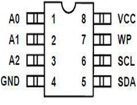
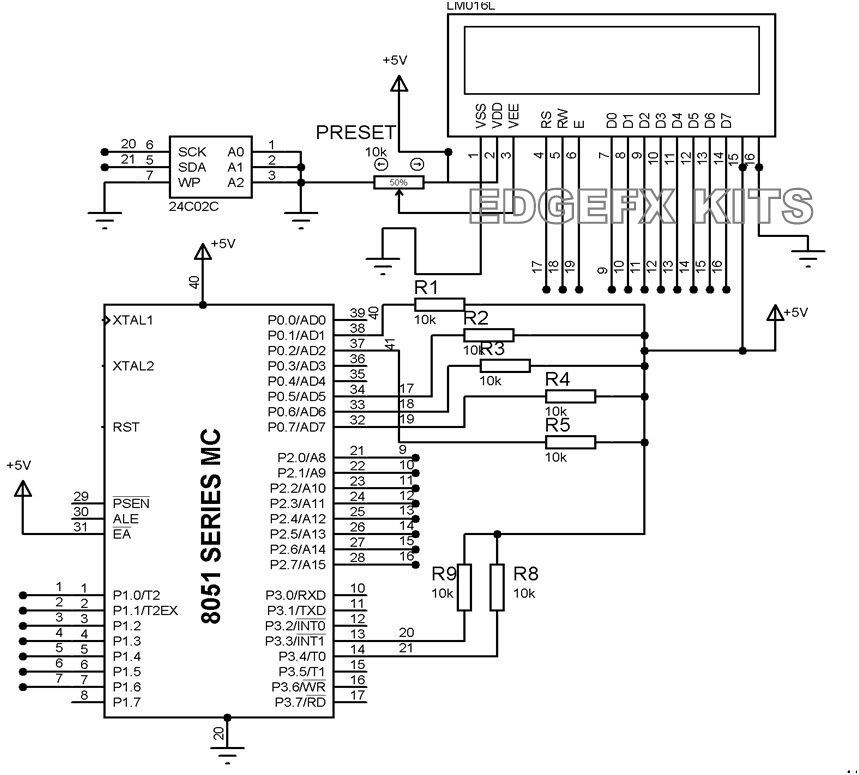
Schematic Diagram Of Interfacing A Serial Eeprom Chip To 32 Bit Download Scientific Diagram

Eeprom Layout Picture Download Scientific Diagram

Block Diagram Of 512 Bit Synchronous Eeprom Download Scientific Diagram

Block Diagram Of Asynchronous 512 Bit Eeprom Download Scientific Diagram
How Eeprom Memory Device Works Discuss The Applications And Features

Eeprom Program Cell Schematic And Cell Layout Showing Cross Coupled Download Scientific Diagram

Block Diagram Of 512 Bit Synchronous Eeprom Download Scientific Diagram

Microcontroller Block Diagram With It S Base Elements And Internal Download Scientific Diagram

3 Block Diagram Of Fpga Board Download Scientific Diagram

Schematic Diagram Of Interfacing A Serial Eeprom Chip To 32 Bit Download Scientific Diagram